Hardware Integration Antenna Placement
Type to start searching
    GitHub
    GitHub
    • Introduction
    • Quickstart
      • Overview
      • Serial
      • USB-Ethernet
      • Wi-Fi
      • Ethernet
      • Features
      • Interfaces
      • Mechanical
      • Electrical
      • Neutis Module
      • Neutis Developer Board
      • Overview
      • Power on sequence
      • Schematics/3D model
      • PCB Design Guide
      • Antenna Placement
        • Recommended area for antenna
        • Polygon cutout for an antenna in Neutis Developer board
      • FEL mode
      • Allwinner H5
      • Audio
      • Bluetooth
      • Camera
      • External Interrupt
      • GPIO
      • HDMI
      • I2C
      • OTA update
      • PWM
      • Secure Chip
      • SPI
      • SPI LCD display
      • UART
      • WiFi Access Point
      • Why Yocto?
      • Build your own Linux OS
      • Device Tree
      • What is Neutis Flasher?
      • Neutis Flasher GUI
      • Neutis Flasher CLI
    • Recommended area for antenna
    • Polygon cutout for an antenna in Neutis Developer board
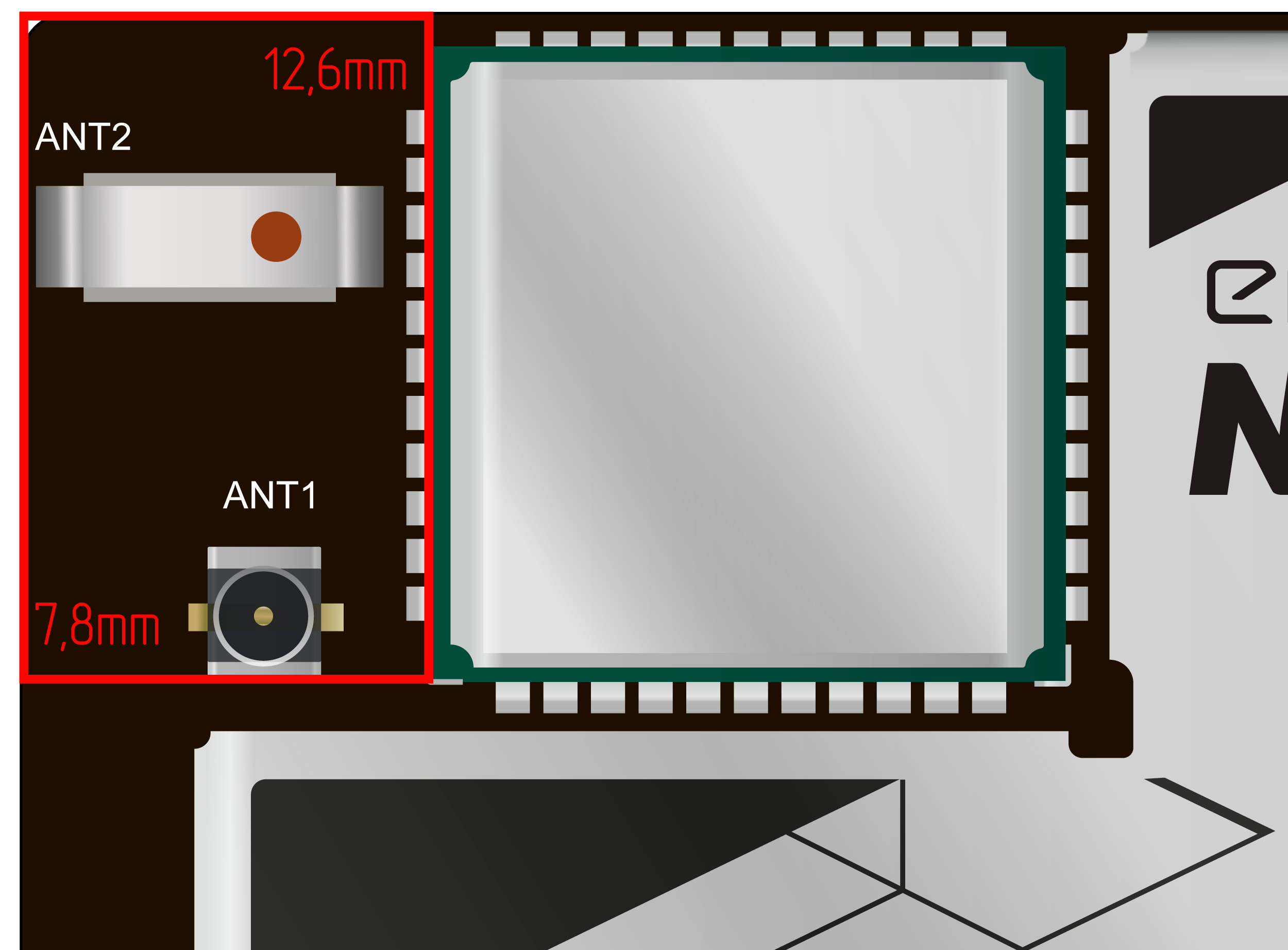
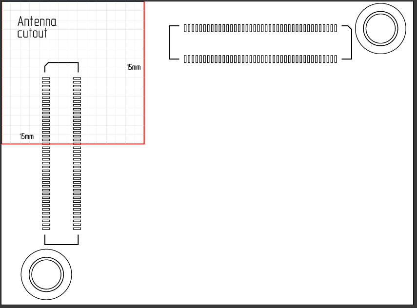
    edit

    Antenna Placement

    Recommended area for antenna


    Warning

    Do not place any routing and copper elements under this area. Use polygon cutout here or place Neutis close to your board edge.

    Polygon cutout for an antenna in Neutis Developer board


    Previous PCB Design Guide
    Next FEL mode
    2018 Emlid.com